




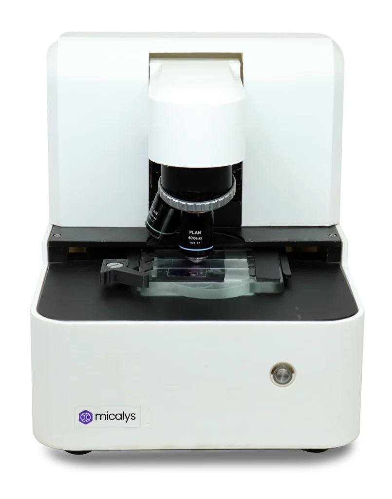


The Invisible Architect: Why Your Smartphone Exists Because of a Microscope
We often view our smartphones as miracles of modern engineering, sleek devices that connect us to the entire world with a simple tap. Yet, beneath the glass and aluminum casing lies a world of complexity so minute that it is entirely invisible to the naked eye. The smartphone in your pocket is not just a triumph of software; it is a masterpiece of materials science, made possible only because of the evolution of microscopy.
Without the ability to visualize, analyze, and manipulate structures at the nanometer scale, the semiconductor industry would not exist as we know it. In this blog, we explore the symbiotic relationship between microscopy and semiconductor manufacturing, revealing why every chip powering your device owes its existence to rigorous inspection processes. This evolution of microscopy has transformed how we build electronics. From the initial design phase to the final assembly, the role of high-end inspection is the backbone of the tech world.
The Foundation of Modern Electronics
At the heart of every smartphone is the semiconductor chip—a tiny silicon wafer packed with billions of transistors. Creating these intricate components requires extreme precision that only modern microscopy can provide. The transition from bulky, unreliable electronics to the powerful, pocket-sized devices we use today was driven by advancements in microscopy and high-precision imaging tools. Without high-resolution microscopy, the semiconductor manufacturing sector could not achieve the required density of each chip’s circuit.
From Vacuum Tubes to Nanometer Circuits
Decades ago, electronics were built using large, visible components. As demand grew for faster, smaller, and more efficient devices, engineers needed to shrink the circuit design. This miniaturization was only achievable by understanding how materials behave at microscopic levels. Optical microscopy served as the foundational tool for early development, allowing engineers to see the physical layout of the circuit and verify the integrity of the manufacturing processes. Through optical microscopy, we established the first standards for quality control in high-tech environments, setting the stage for the hyper-complex chip architectures we rely on today.
The Critical Role of Microscopy in Semiconductor Manufacturing
The manufacturing of a modern semiconductor chip is an incredibly complex journey, often referred to as a “fab”(fabrication) environment. This process relies heavily on photolithography, a technique that uses light to transfer geometric patterns onto a silicon wafer. If there is even a sub-micron defect in the pattern, the entire chip may fail, leading to significant waste in quality control. Microscopy is the guardian of this entire process, ensuring that the manufacturing workflow remains stable from the first wafer input to the final packaged chip.
Photolithography and the Need for Precision
Photolithography defines the success of semiconductor fabrication. Because the patterns being printed are smaller than the wavelength of visible light, high-end microscopy and advanced inspection systems are essential to ensure the accuracy of these transfers. Every chip requires multiple layers of photolithography, and each layer must undergo meticulous inspection. The application of microscopy here is not just an advantage; it is a necessity for modern semiconductor production. The precision of the optics involved in these tools determines the yield rates of the entire manufacturing plant.
Why Inspection is the Pulse of the Industry
In the world of microelectronics, inspection is not just an optional step; it is the pulse of the manufacturing line. Quality control professionals rely on sophisticated microscopy to identify contaminants, surface irregularities, or structural defects during the production cycle. When a chip undergoes inspection, it is analyzed for microscopic flaws that would otherwise render the entire semiconductor useless. This rigorous inspection phase is where potential faults in the circuit are caught before they reach the consumer.
The Science of Inspection
Modern inspection goes far beyond simple magnification. It involves automated optical inspection (AOI) systems that scan every semiconductor wafer for microscopic flaws. By integrating advanced optics with high-speed imaging, these tools ensure that only the most reliable components make it into the final assembly of your smartphone. Without this rigorous inspection, the high performance you expect from your device would be impossible to maintain at a commercial scale. Quality control is paramount, and microscopy provides the raw data needed for these tools to function correctly, mapping out every feature of the circuit to ensure perfection.
Looking Closer: The Evolution of Imaging Tools
As the industry moves toward 3nm, 2nm, and beyond, traditional optical microscopy is often pushed to its physical limits. This necessitates the use of even more advanced microscopy technologies, including electron and scanning probe methods, to complement traditional optical inspection. These tools are essential for monitoring the integrity of the circuit within the semiconductor. By continuously upgrading our microscopy arsenal, we ensure that the semiconductor industry continues to thrive in the face of increasingly complex challenges.
The Synergy of Optics and Innovation
The integration of specialized optics allows for deeper analysis of the semiconductor wafer. These tools are designed to capture data that can be used to optimize the entire manufacturing pipeline. As we look to the future of electronics, the role of microscopy will only become more critical. We depend on optics to peer into the microscopic world of the chip where every circuit must be perfect. The synergy between high-end optics and high-speed inspection software is what makes the current generation of electronics possible.
Ensuring Quality Control at the Nanoscale
Every smartphone relies on the perfection of the chip. Quality control is the guardrail that ensures billions of transistors work in harmony. By utilizing high-resolution microscopy, manufacturers can detect microscopic particles that might cause a short circuit, saving millions of dollars and ensuring the device in your hand is reliable. Through robust quality control and persistent inspection, the semiconductor industry continues to push the envelope of electronics. This constant attention to detail during manufacturing is exactly why your device remains stable under intense computational loads.
The Future of Semiconductor Inspection
As we move forward, the demand for smaller and faster electronics will increase. This means the reliance on advanced microscopy will only grow. Engineers are constantly developing new tools for inspection that utilize novel optics and high-speed data processing. The next generation of semiconductor devices will depend on our ability to see and manipulate the chip at even smaller scales than we do today. This involves deeper integration of microscopy directly into the manufacturing robotic systems.
Innovation in Manufacturing
The manufacturing process is evolving to include AI-driven inspection protocols that use microscopy data to predict failures before they occur. This predictive quality control is changing how we approach the design of every circuit. With advanced optics and cutting-edge microscopy, we can ensure that every chip meets the highest standards. As we move deeper into the nanoscale, the mastery of microscopy becomes the primary competitive advantage for any electronics manufacturer.
The Unseen Force Driving Progress
The next time you unlock your smartphone, remember the “invisible architect” behind it. Microscopy is the silent force that allows us to master the world of the infinitely small. From the precision required in photolithography to the exhaustive inspection of each semiconductor chip, microscopy remains the essential bridge between theoretical design and physical reality.
At Medprime Technologies, we understand the profound impact that precise imaging and optics can have on scientific and industrial advancement. We are proud to support the innovators who push the boundaries of what is possible, ensuring that the technology of tomorrow is built on the firm foundation of today’s most advanced microscopy solutions. Our commitment to high-quality imaging and inspection tools ensures that the future of electronics remains bright, powered by the incredible power of the microscope. Without the microscope, the digital age would never have dawned, and the innovations of the future would remain unreachable.